Before and After the Reaction
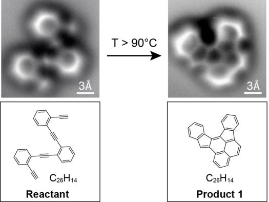
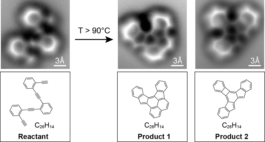
Researchers have for the first time captured atomic-scale images of molecules before and after a chemical reaction–a breakthrough that will help researchers and students better visualize chemistry and could eventually lead to improved electronics.
Traditionally, scientists have to infer how a molecule’s structure changes in a reaction. “In chemistry you throw stuff into a flask and something else comes out, but you typically only get very indirect information about what you have,” lead researcher Felix Fischer, a UC Berkeley assistant professor of chemistry, says in a press release. “You have to deduce that by taking nuclear magnetic resonance, infrared or ultraviolet spectra. It is more like a puzzle, putting all the information together and then nailing down what the structure likely is. But it is just a shadow. Here we actually have a technique at hand where we can look at it and say this is exactly the molecule. It’s like taking a snapshot of it.”
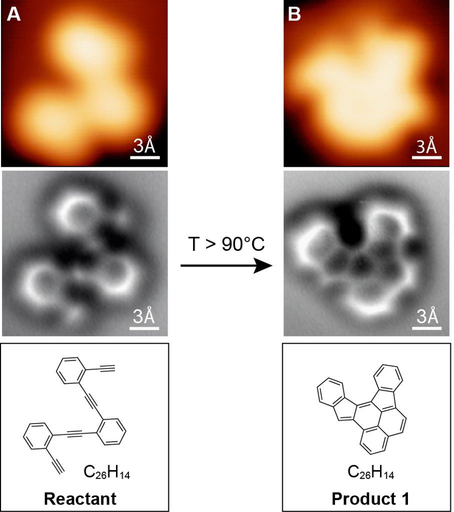
While trying to build new graphene nanostructures, Fischer and his colleagues were able to visualize the exact structure of a molecule–right down to the chemical bonds between atoms–and how that structure changes during a reaction.
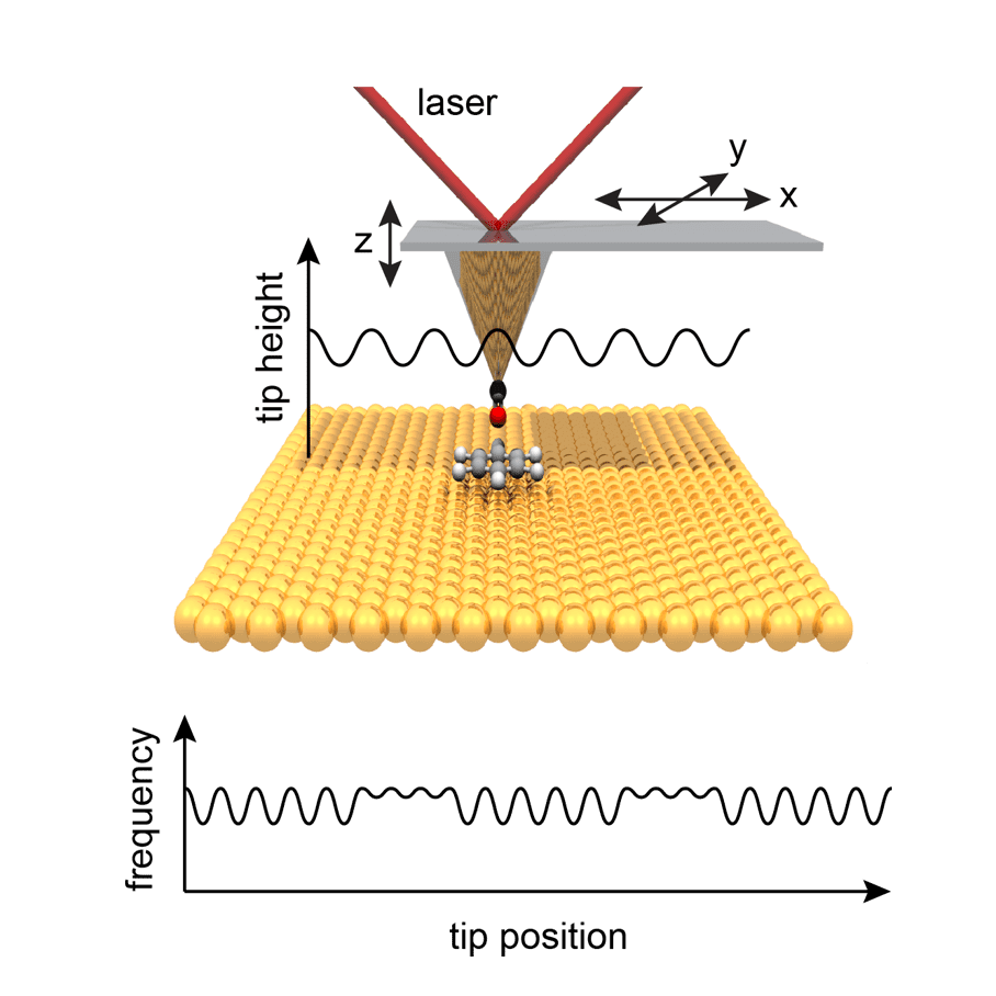
The key? A technique called “noncontact atomic force microscopy.” The ultra-precise carbon molecule tip of a microscope traces the electron bonds between atoms in the molecule, creating an image almost like a leaf rubbing.
Here’s a better look:
Atomic Microscope Image of a Reaction
The implications are both simple (“visualizing chemistry is awesome!”) and elaborate: precisely positioned nanostructures of graphene allow for the construction of absurdly small machines. But to place them precisely, they first have to be visualized. “The atomic force microscope gives us new information about the chemical bond, which is incredibly useful for understanding how different molecular structures connect up and how you can convert from one shape into another shape,” says Michael Crommie, a UC Berkeley professor of physics. “This should help us to create new engineered nanostructures, such as bonded networks of atoms that have a particular shape and structure for use in electronic devices. This points the way forward.”
The images were published in Science Express last week.
Atomic Force Microscope Explained


